
Requirement: To develop and manufacture an automated end of line inspection system for the fault recognition of the wire button style connectors.
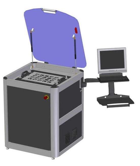
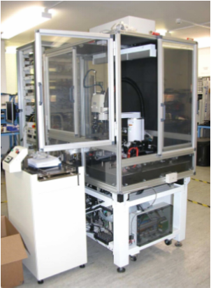
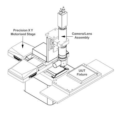 Our solution comprised of a high-resolution vision (camera/lens) system, mounted on a precision X, Y motion stage set-up. A plinth was integrated along with special to type fixtures, very accurately locates the connector to be scanned. The system was housed in a light-tight enclosure that contains a series of controlled light sources, to negate the effect of ambient light on the inspection process. A PXI controller/chassis combination provided PC based control of all aspects of the solution. Integrated motion tools allowed us to scan the vision system over the area covered by the connectors, at the very short focal length required (approx. 12mm from the connector surface). The motion system scanned a pre-determined pattern of steps in X & Y, and the vision system acquires an image at each step. The area captured by the vision system enabled testing of a minimum pattern of 16 buttons/plungers, in a 4 x 4 pattern. Further development allowed us to capture a larger image and reduce total inspection time. The image is then transferred to the vision software and processed against a pre-programmed set of pass/fail criteria, the results of which are buffered until all areas have been scanned. When complete the overall result, Pass or Fail, is displayed as a banner on the system display. System hardwareThe system was based on the PXI platform from National Instruments. A 4 slot PXI chassis houses an embedded PXI-8174 controller, PXI-1422 iMAQ vision card, PXI-7344 Motion control card and a PXI-6508 Digital I/O card for interlock monitoring etc. The software was developed using LabVIEW, the Vision and Motion modules for LabVIEW and the Motion assistant software tools, all from National Instruments. Motion/Vision System The motion system wasconstructed from two 150mm (300mm optional) precision motorised translation stages, mounted to provide travel in both X and Y for the camera/lens system. The stages had a resolution of 10um, which was more than sufficient for this application. A 20mm manual Z adjustment was also provided. The camera selected was a high resolution digital, colour model with suitable lens. System SoftwareThe software algorithm developed is split into 7 main sections. The 7 sections are as follows:
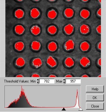
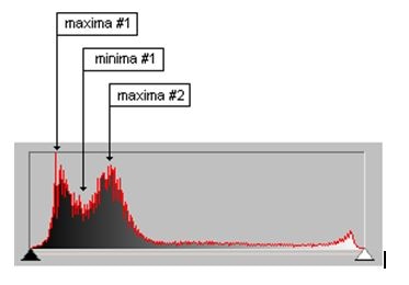
Argument sorting The function of this part of the algorithm simply extracts a 2D array from the 1D argument array being passed in by the controlling software. These arguments include which pins must be tested, and their names. Processing of half lit image This section of the algorithm takes an image of the connector lit with the red led array only. Its function is to isolate the wells on the image, and formulate an array of the wells’ coordinates and radii, which is correlated with the test array formulated in the previous section of the algorithm, ie a sorted array is passed out from this function. A general error condition is raised if the algorithm is unable to isolate a full row or a full column on the grid of wells, as this would mean that there is no reference with which to sort the array. The algorithm is capable of making multiple passes of the image to obtain a sorted array, so if the first thresholding value does not yield the correct number of wells, the algorithm will store those values it has already got, reduce the threshold value and try again up to 5 times. This image shows the ideal illumination for the image lit with the red LED array only.The illumination yields a smoothed histogram which should look like this:
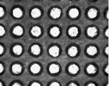
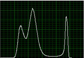
The two maxima must be clearly defined, for a valid thresholding value. This shape of graph is important because the two maxima toward the left of the graph represent the well areas and the substrate area repectively, so the algorithm will threshold somewhere to the left of the 2nd Maxima. Processing of fully lit image In this section of the algorithm, the image with both LED arrays illuminated is used. The image should look like this:
Compare the peak to the peak to the right of the histogram with the half lit histogram, this peak represents potential defect material, and has been enhanced with the second LED array. The Algorithm uses the histogram graph to obtain a new threshold value which falls to the left of the large peak to the right of the histogram graph. A particle filter is introduced also which ignores any particle below a certain threshold. This is a critical point in the code, as the value chosen for this area threshold will drastically affect the results of the tests. The default setting is 90 pixels. This section of the algorithm passes out a binary image from the above threshold / filter operations for the test part of the algorithm. Test 1 This test is for wires appearing outside of the well. A ROI is generated above the well in question using the data in the output sorted array from earlier in the algorithm and a small image extracted from the binary image generated in the fully lit image processing. Each pixel is analysed, if the pixel is high, then its distance is measured from the centre of the well. If that distance is greater than the radius of the well then a variable area is incremented. Each time this variable is incremented then the value of area is checked against a set value area threshold. As soon as area is greater than or equal to area threshold, the pin fails and the test terminates.If this condition is not met then the pin passes. The critical areas here are:
Test 2 This test uses the same binary image as the previous test, and is testing to see if there is a pin present in the well, and does this by looking for high pixels within the radius of the connector which form a single blob. The area of this single blob is measured against a constant value. If the area exceeds the value then the test passes, and fails if not. The current setting for the area is 1500 pixels. Display and report This final section of the algorithm overlays test results onto the image, and compiles a report to pass back to the calling vi. Conclusion:The system met all system requirements. The use of the LabVIEW vision and motion tools enabled a much faster and reliable test solution than the old manual test procedure. Additional software has been added to improve the feature set for the customer who is extremely pleased with the result.
1 Comment
Amfax also integrated an image acquisition system to provide handling with vision. This provided the system with the ability to check the device against an absolute and locate it accurately in X, Y and Theta. We were then able to check for missing devices, devices that were misallocated in their pockets and also for devices that were in the incorrect orientation.
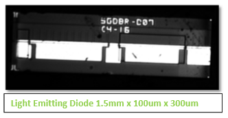
The integration of NI LabVIEW and iMAQ and control of the robot was developed by Amfax to provide a completely interactive environment specifically for handling of opto-electronic devices. The depth of field required to capture the image from the devices is restricted to 150um Temperature controlled test pedestals manufactured from elkanite, a tungsten / copper alloy were used to provide the test bed for the UUT controlled using solid state temperature sensors and Keithley controllers. To allow maintenance of the test head such as replacing Peltier heat pumps the pedestal was mounted on X and Y stages integrated into the assembly. This provided the system with fine adjustment for the UUT location and after replacement the stages could be re-taught to their zero position while not needing to re-teach the robot. The probing assembly was located above the test head and lowered into position via precision stages after the robot had placed the device. The wedge probe design from Pico probe, with kelvin probing incorporated was used for testing the chip. The typical tolerance required to make contact with each mirror was + / - 25um A single mode fibre mounted on an X / Y & Z precession stages was used to align with the wave guide of the device and measure the maximum power once voltage was applied to each mirror using the Pico probe. + / - 5um was required to maintain the sweet spot. The system was housed in a lamina flow filter system mounted on an optically flat, vibration isolated table. The chip trays were fed into the system using a mag handler operated via RS232, the system would request a product to test via an agreed RS232 string sent to the controller, the handler would then take all the steps to place the trays in a position ready for the robot to begin pick and place routine to finally test the devise on the test head |

Our recent workWe provide regular updates on the latest projects we have been working on. Check out our archive to view all of our case studies and user solutions. Archives
April 2018
Categories
All
|
 RSS Feed